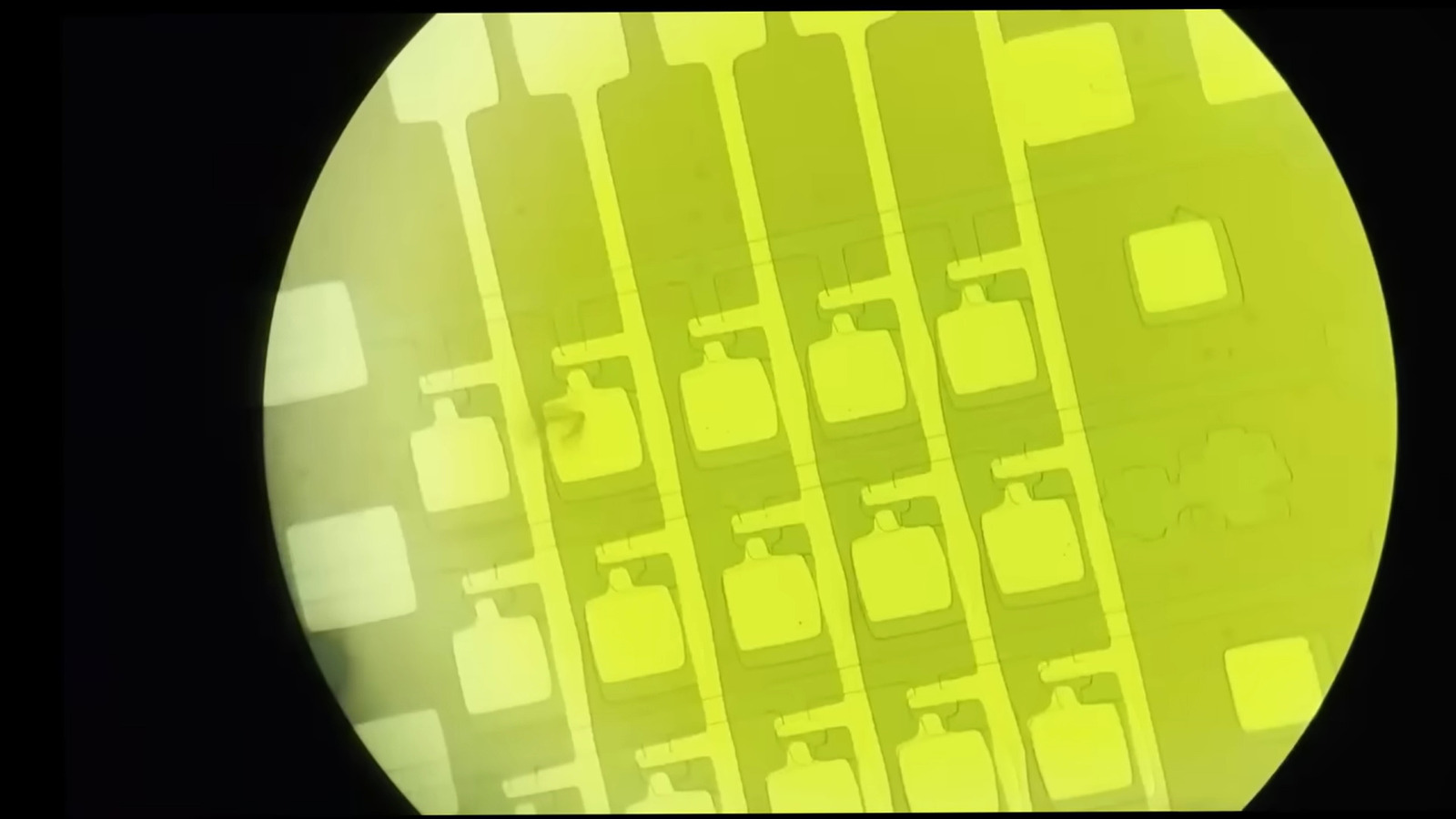

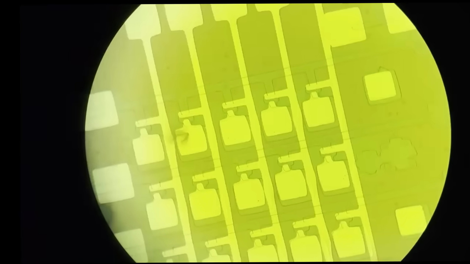
Can you make RAM at home? Technically, yes. One person, YouTuber Dr. Semiconductor, has done it, but it’s unlikely the rest of us are about to get around the current out-of-control RAM prices by cooking up dynamic random access memory (DRAM) chips in the kitchen. His project is impressive precisely because it shows how hard the job is. Even a tiny, experimental memory array requires chemistry, photolithography, high-temperature processing, and electrical testing gear.
In fact, even the first step in Dr. Semiconductor’s RAM-making journey sounds near-impossible for most people. He turned his garden shed into a Class 100 clean room. This means that it has no more than 100 particles of 0.5 microns or larger per cubic foot. Even the “dirtiest” classified clean room, a Class 100,000, is still significantly cleaner than most homes, which have 500,000 to 1 million particles per cubic foot. Most people’s garden sheds likely have even more.
The lab needed to be that clean because the useful features on a RAM chip are microscopic. A speck of dust that would be invisible on your desk would be disastrous in such an environment. Commercial semiconductor manufacturers spend billions on fabs because producing working chips depends on precisely controlling things like dust particles, temperature, humidity, and vibration.
Dr. Semiconductor’s homemade version was not a full RAM stick, nor anything close to a commercial memory chip. He designed a 5-by-4 array: just 20 RAM cells, each made from a transistor-capacitor pair. That’s tiny compared with modern memory devices, which can contain billions of cells, but it’s an extraordinary achievement for a shed-based lab.
How to build a RAM chip
Dr. Semiconductor created DRAM, the most common type of RAM used in modern devices. DRAM enables operating systems and applications to temporarily store and access data quickly, making it a key factor in system performance and responsiveness. It stores data in a deceptively simple way. Each bit lives in a tiny memory cell made from a transistor and a capacitor. The capacitor holds electrical charge, representing a 1 or a 0, while the transistor acts like a gate that allows the cell to be read or written. The catch is that capacitors leak. Left alone, the charge fades, so DRAM has to be refreshed again and again before the stored information decays.
The process began with silicon wafer pieces, cut down using a diamond scribe. The chips were cleaned with solvents to remove organic residue and surface contamination. From there, the work moved into the rhythm of semiconductor fabrication: grow or deposit a layer, pattern it, etch it, modify the silicon, strip material away, and repeat. To form the active transistor regions, the YouTuber used phosphorus doping, applying doped spin-on glass and heating the chips at high temperatures so dopant atoms could diffuse into the silicon.
He then used photolithography to define the tiny structures needed for the DRAM cells. In that process, the chip is coated with photoresist, a light-sensitive material that works like a temporary stencil. After exposure and development, some areas are protected while others are left open for etching or doping. Aluminum was then deposited for contacts and capacitor plates using a sputtering system, a vacuum-based technique that blasts atoms from a metal target onto the chip surface. Finally, the remaining photoresist was stripped away to reveal the completed structures.
Testing the finished product
In order to test the array, Dr. Semiconductor couldn’t just plug it into a motherboard and see if a computer recognized it, like you could with a product from a major RAM brand. He had to test it the way semiconductor devices are tested in a lab: one tiny structure at a time, using instruments sensitive enough to measure what ordinary wires and a multimeter can’t. That meant using a semiconductor parameter analyzer and micro-manipulators fitted with extremely fine probe tips. The probes let him touch specific contact pads on the chip, apply voltages, and measure how the homemade transistors and capacitors responded. Could the transistor act as a switch? Could the capacitor store charge? And would the cell hold that charge long enough to be read back?
The answer was yes — but with a very large asterisk. The homemade cells behaved like working DRAM cells, which is an astonishing result for a shed-built semiconductor process. They could be written, charged, and measured, but they also leaked charge far faster than commercial memory. The cells needed refreshing in about 2 milliseconds, compared with the roughly 64-millisecond refresh window commonly associated with DRAM. That means they would need to be refreshed more than 30 times as often.
It means that this homemade RAM isn’t yet usable in the everyday sense. However, now that he’s built a functioning DRAM cell array from scratch, Dr. Semiconductor plans to make a much larger array that can be linked to a computer. Crucially, this intrepid YouTuber proved RAM can be made at home. He also proved why nobody else does.

Stephan is the sports journalist for the Maple Grove Report.