
IBM’s NanoStack sub-1nm chip arrives
IBM
Follow ZDNET: Add us as a preferred source on Google.
ZDNET’s key takeaways
- IBM’s sub-1-nanometer NanoStack architecture holds almost 100 billion transistors on a chip.
- These chips are cheaper to run and more powerful than previous generations.
- NanoStack technology will be great for deploying AI workloads.
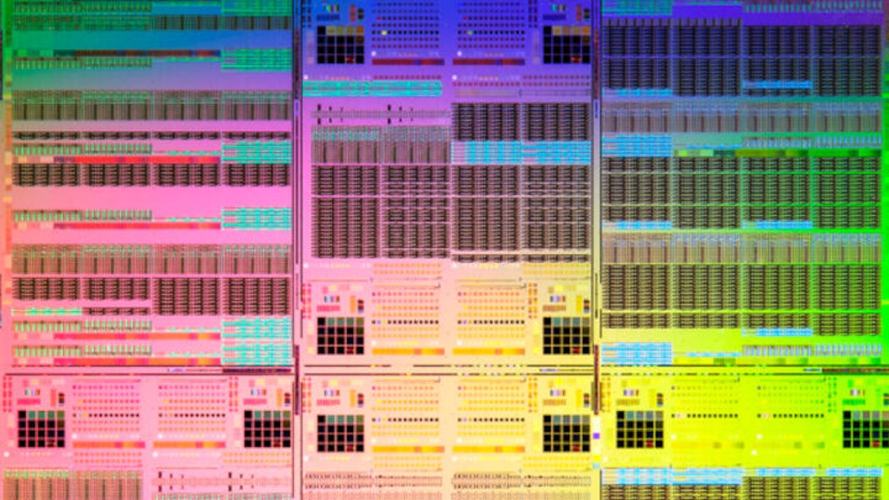
TSMC, Intel, and Samsung have all been pushing to produce low‑single‑nanometer chips in the next two years, while planning to produce sub-nanometer chips sometime by decade’s end. That race may be over, however, even before it began. IBM unveiled what it says is the world’s first sub-1-nanometer chip technology based on a new 3D NanoStack transistor architecture at the 0.7 nm — or 7 angstrom — node.
The research device, introduced ahead of VLSI 2026, is designed to pack nearly 100 billion transistors on a fingernail‑size die, roughly doubling the density of IBM’s earlier 2-nm test chip, first shown in 2021. Today, the smallest, most powerful chips top out at about 80 billion transistors.
Also: Why your RAM options cost 4X more now than last year – even legacy tech prices aren’t immune
What’s so important about teeny-tiny chips? They’re valuable because they let you pack more transistors into a given area while using less power, which translates into higher performance, lower energy use, and lower cost per unit of compute. In case you’ve been living under a rock, AI demands low-power, cheap chips. There’s a huge market for these chips.
From nanosheet to ‘nanostack’
At the heart of the announcement is NanoStack. This is a three‑dimensional, nanosheet‑based transistor design that scales vertically, or along the z‑axis, by stacking and staggering CMOS devices. Unlike today’s nanosheet architectures, which IBM also pioneered and which are being adopted by leading foundries at 3 nm and 2 nm, NanoStack bonds two nanosheet transistors into a single vertical structure, with each tier optimized independently and contacted from opposite sides.
Each transistor in the demonstrated structure uses three sub-5 nm‑thick nanosheets, about “15 silicon atoms” across, separated by roughly 9 nm spacers. Two such devices are then bonded vertically using an ultra‑thin dielectric process IBM describes as a key innovation. Because the top and bottom devices can use different channel materials, dielectrics, and metals, IBM argues NanoStack is less a single trick and more a transistor platform that can be extended through multiple generations: 7 angstrom (Å), 5 Å, 3 Å, and potentially down to 1 Å in its internal roadmap.
Also: How much RAM does your PC need in 2026? My advice after using Windows and Mac for years
An angstrom, by the by, is one ten-billionth of a meter. In terms of chips, an angstrom is a tenth of a nanometer.
“This is the world’s first sub‑1 nanometer chip technology with a new transistor architecture,” said Jay Gambetta, Director of IBM Research and IBM Fellow, during a press briefing. “We’re not just making smaller transistors, we’re reinventing how chips are built to deliver dramatically more power and energy efficiency.”
Projected gains: performance, efficiency, and SRAM density
IBM is positioning the 0.7 nm technology as a meaningful step beyond today’s nanosheet nodes rather than just another incremental shrink. Based on internal benchmarking against its 2 nm node, the company said its new chips will deliver up to 50% higher performance at the same power, or up to 70% lower power for the same performance.
Big Blue also highlighted a 40% improvement in the scaling of static random-access memory (SRAM) cell area relative to its 2 nm technology. This is a change IBM described as a “step the industry hasn’t seen in over a decade” and one that could be particularly important for AI accelerators that live or die on on‑chip memory bandwidth.
In the lab, IBM said it has experimentally validated the architecture with ultra‑thin dielectric bonding in a CMOS process, demonstrated dual‑channel engineering across the stacked devices, and shown functional CMOS inverters with expected switching behavior. “Together, these results confirm the nanostack technology can be physically built and supports real computation,” the company said in its press materials.
Angstrom‑class scaling, High‑NA EUV, and materials
IBM is explicit that “0.7 nm” and “7 angstrom” should be read as generational node names, not literal gate lengths or pitches, in line with the broader industry trend of decoupling node labels from specific physical dimensions. Internally, the company said it benchmarked NanoStack’s critical dimensions—such as gate pitches and contacted gate pitch—against a projected 1 nm‑class node, then pushed scaling by going vertical.
To get there, the Albany research line leans heavily on advanced lithography and materials work. IBM and partners in New York, including ASML, Lam Research, Tokyo Electron, and SCREEN, are already installing a High Numerical Aperture EUV (High‑NA EUV) tool, the company calls “essential for the future of logic scaling,” and are evaluating new metal‑oxide resists for patterning at angstrom‑class nodes. On the device side, NanoStack’s separation of top and bottom transistors opens the door to introducing new channel materials and dielectrics on a per‑tier basis without having to qualify them across an entire planar CMOS stack.
Also: I compared virtual RAM with real RAM on my Windows PC – here’s what the numbers told me
According to Huiming Bu, IBM’s VP of silicon technology R&D, NanoStack is a new paradigm. It’s moving chips to scaling fully into three dimensions and giving the industry at least “another decade” of logic advances as it crosses from nanometers into angstroms.
Don’t get too excited quite yet, though. Historically, introducing any genuinely new material into high‑volume CMOS has taken well over a decade. However, IBM argues NanoStack’s partitioned architecture can reduce that friction. Still, university device researchers are already approaching IBM to explore new materials within the architecture.
AI, data centers, and commercialization timeline
Although the 0.7 nm chip demonstrated today is a research project, IBM is already tying the work directly to AI and cloud roadmaps. Gambetta and Bu both framed the performance‑per‑watt gains as crucial to accommodating runaway AI demand without equally runaway power bills, particularly in data centers where electricity and cooling are now defining constraints.
“Everyone demands more performance, but no one wants to pay the bill for the power,” Bu said. “This new innovation can improve performance by 50% compared to the best available chip today, and at the same time can reduce power by 70% if you choose to manage your power in that computing, which is a very critical component for AI.” The 40% SRAM density bump could also help architects push caches and on‑die memory closer to compute units, cutting data movement overhead in training and inference workloads.
IBM stressed that NanoStack is a generic logic technology. It’s not a one-off or special‑purpose structure. IBM expects NanoStack to eventually underpin CPUs, GPUs, mobile SoCs, and SRAM arrays. While it is currently focused on bringing its nanosheet‑based 2 nm process into manufacturing with Japanese foundry partner Rapidus, IBM said NanoStack is intended to replace nanosheet as the mainstream leading‑edge architecture starting at the sub‑1 nm node.
With that caveat, the company is still talking about selling its chips in the future. Drawing on its history of transferring nanosheet IP and other device innovations to commercial foundries, IBM said it sees a path to production use of NanoStack at a sub‑1 nm node “in as early as the next 5 years.”